


Surface Pro 3 landscape docking station teardown

[Skip ahead to part 2 for info on the 40-pin connector]
Being a Surface fanatic, I wanted to see what was inside the Surface Pro 3 docking station:

Tools:
#0 Philips screwdriver
#00 Philips screwdriver
1/8” flat screwdriver
pliers
Pentalobe screwdriver (needed for non-destructive method)
Dremel or similar cutting tool (needed for destructive method shown)
Disclaimer:
Opening your Microsoft Surface Pro 3 will void your warranty. You should take every precaution when tearing apart any consumer electronic device. Even though the Surface Pro 3 dock operates at 12V, you should be careful to keep metal bits and tools away to not short out anything. If you are not familiar with the safety aspects of working with electronic projects, do not attempt this teardown. Ifixit has a good safety guide for electronic teardowns and repairs.
Part 1 – Removing fasteners
Flip over and pull off bottom sticker

Remove 5 pentalobe screws on the back of the dock
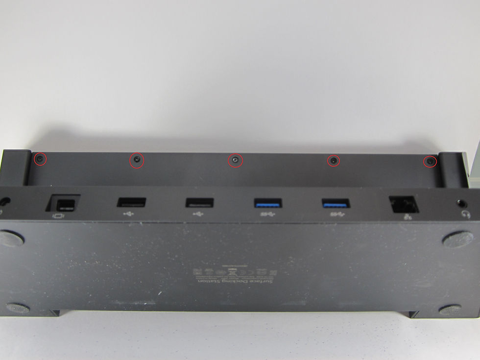
Here is one of the screws up close

If you don’t have a Pentalobe screwdriver, use a Dremel cutting wheel or similar tool to cut a slit in the screws then remove with regular slot screwdriver

Pry off front cover – the cover is stuck on with adhesive so it will take a little force to pry off

It is best to pry off with the docking clamp mechanism opened so it won’t jam

Take a minute to check out the design and operate the docking clamp a few times to see everything work; then remove the 26 screws circled in red

Pry metal guide free

Remove bearings and free cables from white plastic guide

Remove 12 screws

Pry off bottom cover

Part 2 – Separate board from chassis and cable assembly
Free circuit board from chassis by gently prying up at corners.

Push in USB retainer tabs and free the plug – wow its a standard type-A plug!

Free 7-pin power header (looks like a standard Foxconn part)

Free 3-pin DisplayPort power header with slot screwdriver or fingernails (it looks like a wake-on-lan connector)

Remove 4 tiny DisplayPort screws on underside of board with #00 Philips driver

Free DisplayPort receptacle and re-install 4 screws so they don’t get lost

Free at last!

If you are building the 3-in-1 Dock put the circuit board back into that last piece of the plastic housing.
Part 3 – Separate 40-pin charging connector

Remove 2 screws

Pry off cover to reveal 4 more screws and remove them

Pull each cable end through plastic opening one at a time: power, USB, then DisplayPort to free the cable assembly. I wonder how 40 tiny wires get soldered inside that fancy connector?
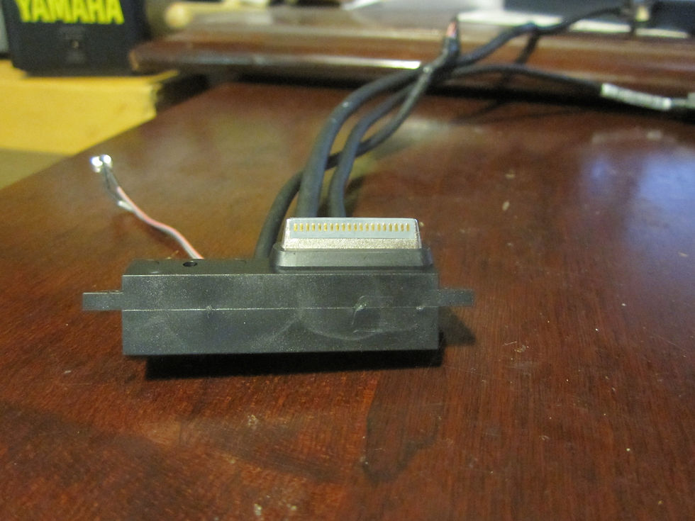
If you are building the 3-in-1 Dock, Re-connect the cable to the circuit board and stop
Part 4 – Examining the board (Optional)
Remove 6 screws to dislodge the main RF shields

Lift the individual square shields up by prying with small screwdriver at corners

Cut through the “+” shaped frame of the individual RF shields to expose the integrated circuits underneath
Left side
Under top left shield
Conexant CX20772 audio chip
LM352 DC-DC converter to power audio chip
Under bottom right shield
SMSC USB5537B 7-port hub (4 USB 3.0, 3 USB 2.0)
Atmel H340 8-pin serial EEPROM chip?
AP2176 8-pin power switch for USB 3.0 downstream port

Middle
2 more AP2176 8-pin power switches for USB 3.0 downstream ports
NXP LPC811 16-pin microcontroller – for tablet charging circuit?
Undetermined tiny 8-pin chip with markings “C 40 AA” next to the LPC811


Right side
Under shield
2 NCP3170A PAZZ 8-pin buck voltage regulators
Undetermined IC with markings “43A097U 21305SQ”
2 NTMS4177P PE06 8-pin power mosfet chips for tablet charging?
3540 8-pin voltage regulator (3.3v 500mA for DisplayPort?)
Undetermined IC with markings “4C55N RAMOE” next to large capacitor – probably some sort of power regulator or mosfet package
Undetermined tiny 8-pin IC with markings “ACH” next to DisplayPort power connector

Underside – Realtek 8153AM Gigabit Ethernet and two buffer chips

Conclusion
The clamp mechanism is a thing of beauty but I can’t believe how many fasteners there are! The circuit board is surprisingly sparse with several open pad areas. It looks like one of the open pad areas is for a 48-pin IC connected to DisplayPort. Perhaps in one design there was a built-in DisplayPort repeater chip. There is a signal insertion loss at the tablet -> 40-pin connector and another loss at the dock passthrough port so that’s a lot of loss to deal with.
The board looks like it is 6 or 8 layers and being so sparsely populated, its surprising to see the Realtek 8153 chipset on the bottom given the extra manufacturing expense. There is probably a good reason for it – my guess is trying to separate the USB 3.0 high-frequency bits from the GigE as much as possible. The cable assembly is wonderful in that it allows a very modular design for everything; it breaks out from the 40-pin charging connector into mini-DisplayPort, 3-pin DisplayPort power connector, USB 3.0 type-A plug, a 7-pin power connector, and a charging indicator LED. Just imagine what else can be created with this cable…
References
Although posted after I did my teardown, Fred_Com’s teardown to fix DisplayPort issues is quite helpful: http://www.surfaceforums.net/threads/surface-3-dock-disassembly-displayport-sync-issue-fix.14530/
Back to the main blog https://dancharblog.wordpress.com

Comments